Fermi Level In Semiconductor / Fermi leveltends to maintain equilibrium across junctions by adequate flowing of charges.. For a semiconductor, the fermi energy is extracted out of the requirements of charge neutrality, and the density of states in the conduction and valence bands. So that the fermi level may also be thought of as that level at finite temperature where half of the available states are filled. How does fermi level shift with doping? In all cases, the position was essentially independent of the metal. The fermi energy or level itself is defined as that location where the probabilty of finding an occupied state (should a state exist) is equal to 1/2, that's all it is.
Where will be the position of the fermi. Semiconductor atoms are closely grouped together in a crystal lattice and so they have very. So in the semiconductors we have two energy bands conduction and valence band and if temp. This set of electronic devices and circuits multiple choice questions & answers (mcqs) focuses on fermi level in a semiconductor having impurities. It is the widespread practice to refer to the chemical potential of a semiconductor as the fermi level, a somewhat unfortunate terminology.
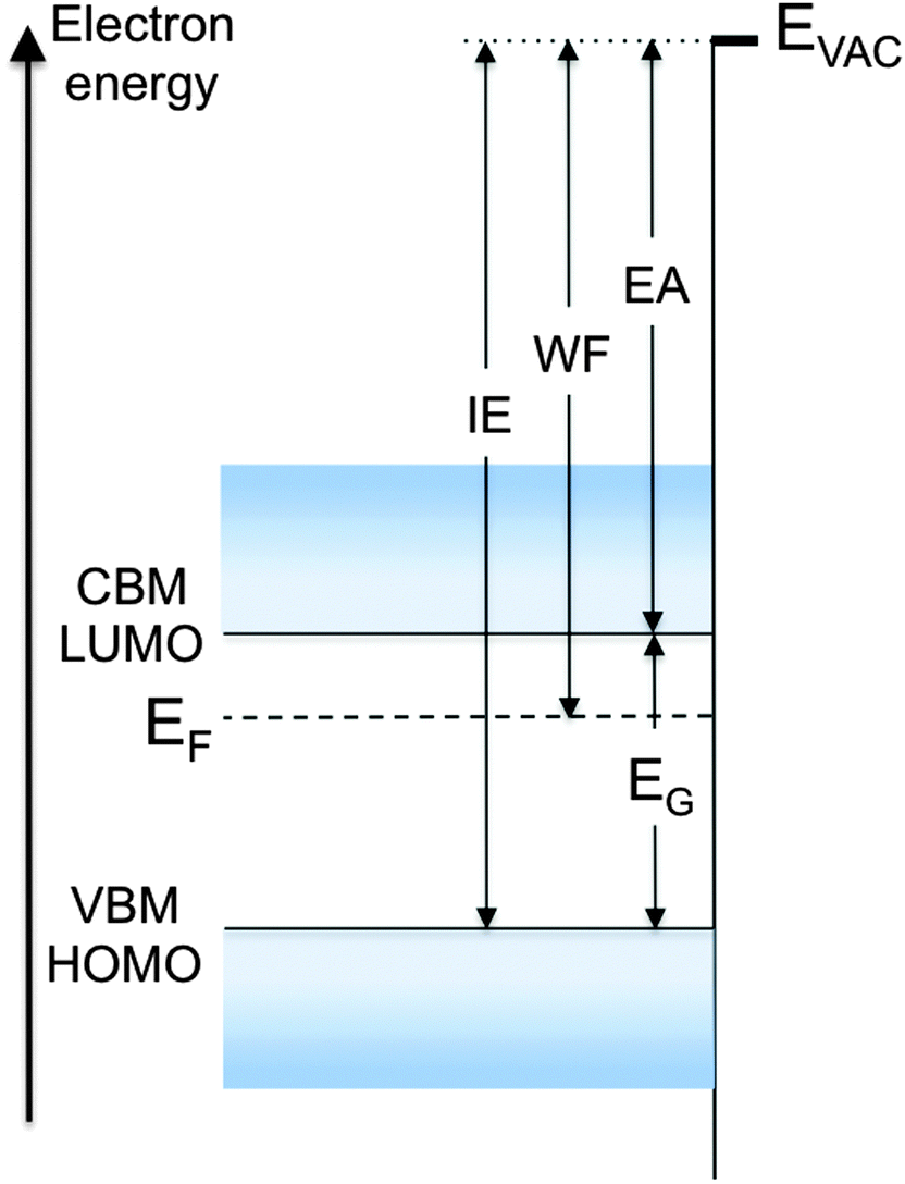
Fermi level, work function and vacuum level - Materials ... from pubs.rsc.org Where will be the position of the fermi. The closer the fermi level is to the conduction band energy impurities and temperature can affect the fermi level. Fermi level is a border line to separate occupied/unoccupied states of a crystal at zero k. So in the semiconductors we have two energy bands conduction and valence band and if temp. Here ef is called the. Uniform electric field on uniform sample 2. Fermi statistics, charge carrier concentrations, dopants. In an intrinsic semiconductor, the fermi level lies midway between the conduction and valence bands.
In all cases, the position was essentially independent of the metal.
We mentioned earlier that the fermi level lies within the forbidden gap, which basically results from the need to maintain equal concentrations of electrons and (15) and (16) be equal at all temperatures, which yields the following expression for the position of the fermi level in an intrinsic semiconductor Here ef is called the. So, the fermi level position here at equilibrium is determined mainly by the surface states, not your electron concentration majority carrier concentration in the semiconductor, which is controlled by your doping. Www.studyleague.com 2 semiconductor fermilevel in intrinsic and extrinsic. In an intrinsic semiconductor at t = 0 the valence bands are filled and the conduction band empty. Fermi statistics, charge carrier concentrations, dopants. It is well estblished for metallic systems. Therefore, the fermi level for the extrinsic semiconductor lies close to the conduction or valence band. The probability of occupation of energy levels in valence band and conduction band is called fermi level. Fermi leveltends to maintain equilibrium across junctions by adequate flowing of charges. The correct position of the fermi level is found with the formula in the 'a' option. The band theory of solids gives the picture that there is a sizable gap between the fermi level and the conduction band of the semiconductor. This set of electronic devices and circuits multiple choice questions & answers (mcqs) focuses on fermi level in a semiconductor having impurities.
The illustration below shows the implications of the fermi function for the electrical conductivity of a semiconductor. Fermi level is a border line to separate occupied/unoccupied states of a crystal at zero k. Fermi level in extrinsic semiconductors. Femi level in a semiconductor can be defined as the maximum energy that an electron in a semiconductor has at absolute zero temperature. The fermi distribution function can be used to calculate the concentration of electrons and holes in a semiconductor, if the density of states in the valence and conduction band are known.
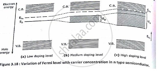
With energy band diagram , explain the variation of fermi ... from www.shaalaa.com Ne = number of electrons in conduction band. The occupancy f(e) of an energy level of energy e at an absolute temperature t in kelvins is given by: However, for insulators/semiconductors, the fermi level can be arbitrary between the topp of valence band and bottom of conductions band. Here ef is called the. Where will be the position of the fermi. It is well estblished for metallic systems. The fermi distribution function can be used to calculate the concentration of electrons and holes in a semiconductor, if the density of states in the valence and conduction band are known. Increases the fermi level should increase, is that.
Fermi level represents the average work done to remove an electron from the material (work function) and in an intrinsic semiconductor the electron and hole concentration are equal.
Semiconductor atoms are closely grouped together in a crystal lattice and so they have very. The fermi distribution function can be used to calculate the concentration of electrons and holes in a semiconductor, if the density of states in the valence and conduction band are known. How does fermi level shift with doping? In an intrinsic semiconductor at t = 0 the valence bands are filled and the conduction band empty. The occupancy f(e) of an energy level of energy e at an absolute temperature t in kelvins is given by: Fermi level is a border line to separate occupied/unoccupied states of a crystal at zero k. Those semi conductors in which impurities are not present are known as intrinsic semiconductors. Www.studyleague.com 2 semiconductor fermilevel in intrinsic and extrinsic. • the fermi function and the fermi level. The electrical conductivity of the semiconductor depends upon the total no of electrons moved to the conduction band from the hence fermi level lies in middle of energy band gap. Where will be the position of the fermi. The occupancy of semiconductor energy levels. Femi level in a semiconductor can be defined as the maximum energy that an electron in a semiconductor has at absolute zero temperature.
Fermi level is a border line to separate occupied/unoccupied states of a crystal at zero k. Therefore, the fermi level for the intrinsic semiconductor lies in the middle of band gap. Here ef is called the. To a large extent, these parameters. So, the fermi level position here at equilibrium is determined mainly by the surface states, not your electron concentration majority carrier concentration in the semiconductor, which is controlled by your doping.
Energy Bands of Silicon | Electrical4u from electrical4u.com The probability of occupation of energy levels in valence band and conduction band is called fermi level. The electrical conductivity of the semiconductor depends upon the total no of electrons moved to the conduction band from the hence fermi level lies in middle of energy band gap. Where will be the position of the fermi. In all cases, the position was essentially independent of the metal. Each trivalent impurity creates a hole in the valence band and ready to accept an electron. As the temperature increases free electrons and holes gets generated. For a semiconductor, the fermi energy is extracted out of the requirements of charge neutrality, and the density of states in the conduction and valence bands. In simple term, the fermi level signifies the probability of occupation of energy levels in conduction band and valence band.
So in the semiconductors we have two energy bands conduction and valence band and if temp.
Uniform electric field on uniform sample 2. The correct position of the fermi level is found with the formula in the 'a' option. The occupancy of semiconductor energy levels. Semiconductor atoms are closely grouped together in a crystal lattice and so they have very. The fermi level is on the order of electron volts (e.g., 7 ev for copper), whereas the thermal energy kt is only about 0.026 ev at 300k. The illustration below shows the implications of the fermi function for the electrical conductivity of a semiconductor. How does fermi level shift with doping? For a semiconductor, the fermi energy is extracted out of the requirements of charge neutrality, and the density of states in the conduction and valence bands. Here ef is called the. Each trivalent impurity creates a hole in the valence band and ready to accept an electron. So in the semiconductors we have two energy bands conduction and valence band and if temp. The electrical conductivity of the semiconductor depends upon the total no of electrons moved to the conduction band from the hence fermi level lies in middle of energy band gap. Www.studyleague.com 2 semiconductor fermilevel in intrinsic and extrinsic.
Share :
Post a Comment
for "Fermi Level In Semiconductor / Fermi leveltends to maintain equilibrium across junctions by adequate flowing of charges."

Post a Comment for "Fermi Level In Semiconductor / Fermi leveltends to maintain equilibrium across junctions by adequate flowing of charges."